
 Search
 Feedback
 About UniCat
  Help
Help News
News
| Listing 1 - 5 of 5 |
Sort by
|

ISBN: 0126738424 9786611057114 1281057118 0080538185 9780126738421 9780080538181 9781281057112 6611057110 Year: 1999 Publisher: San Diego Academic Press
Abstract | Keywords | Export | Availability | Bookmark
 Loading...
Choose an application
- Reference Manager
- EndNote
- RefWorks (Direct export to RefWorks)
This book describes the operation of a particular technique for the production of compound semiconductor materials. It describes how the technique works, how it can be used for the growth of particular materials and structures, and the application of these materials for specific devices. It contains not only a fundamental description of the operation of the technique but also contains lists of data useful for the everyday operation of OMVPE reactors. It also offers specific recipes that can be used to produce a wide range of specific materials, structures, and devices.Key Features*
Compound semiconductors --- Metal organic chemical vapor deposition --- Semiconductors --- Metal organic vapor phase epitaxy --- Metallorganic vapor phase epitaxy --- MOCVD (Vapor deposition) --- MOVPE (Vapor deposition) --- OMCVD (Vapor deposition) --- OMVPE (Vapor deposition) --- Organo-metal vapor phase epitaxy --- Organometallic chemical vapor deposition --- Organometallic vapor phase epitaxy --- Chemical vapor deposition --- Compound semiconductors. --- Metallic organic chemical vapor deposition.
Book
Year: 2021 Publisher: Basel, Switzerland MDPI - Multidisciplinary Digital Publishing Institute
Abstract | Keywords | Export | Availability | Bookmark
Loading...Choose an application
- Reference Manager
- EndNote
- RefWorks (Direct export to RefWorks)
Owing to their unique characteristics, direct wide bandgap energy, large breakdown field, and excellent electron transport properties, including operation at high temperature environments and low sensitivity to ionizing radiation, gallium nitride (GaN) and related group III-nitride heterostructures proved to be enabling materials for advanced optoelectronic and electronic devices and systems. Today, they are widely used in high performing short wavelength light emitting diodes (LEDs) and laser diodes (LDs), high performing radar, wireless telecommunications, as well ‘green’ power electronics. Impressive progress in GaN technology over the last 25 years has been driven by a continuously growing need for more advanced systems, and still new challenges arise and need to be solved. Actually, lighting industry, RF defene industry, and 5G mmWave telecommunication systems are driving forces for further intense research in order to reach full potential of GaN-based semiconductors. In the literature, there is a number of review papers and publications reporting technology progress and indicating future trends. In this Special Issue of Electronics, eight papers are published, the majority of them focusing materials and process technology of GaN-based devices fabricated on native GaN substrates. The specific topics include: GaN single crystalline substrates for electronic devices by ammonothermal and HVPE methods, Selective – Area Metalorganic Vapour – Phase Epitaxy of GaN and AlGaN/GaN hetereostructures for HEMTs, Advances in Ion Implantation of GaN and Related Materials including high pressure processing (lattice reconstruction) of ion implanted GaN (Mg and Be) and III-Nitride Nanowires for electronic and optoelectronic devices.
Technology: general issues --- GaN HEMT --- self-heating effect --- microwave power amplifier --- thermal impedance --- thermal time constant --- thermal equivalent circuit --- GaN --- crystal growth --- ammonothermal method --- HVPE --- ion implantation --- gallium nitride --- thermodynamics --- ultra-high-pressure annealing --- diffusion --- diffusion coefficients --- molecular beam epitaxy --- nitrides --- laser diode --- tunnel junction --- LTE --- AlN --- AlGaN/GaN --- interface state density --- conductance-frequency --- MISHEMT --- gallium nitride nanowires --- polarity --- Kelvin probe force microscopy --- selective area growth --- selective epitaxy --- AlGaN/GaN heterostructures --- edge effects --- effective diffusion length --- MOVPE --- nanowires --- AlGaN --- LEDs --- growth polarity --- GaN HEMT --- self-heating effect --- microwave power amplifier --- thermal impedance --- thermal time constant --- thermal equivalent circuit --- GaN --- crystal growth --- ammonothermal method --- HVPE --- ion implantation --- gallium nitride --- thermodynamics --- ultra-high-pressure annealing --- diffusion --- diffusion coefficients --- molecular beam epitaxy --- nitrides --- laser diode --- tunnel junction --- LTE --- AlN --- AlGaN/GaN --- interface state density --- conductance-frequency --- MISHEMT --- gallium nitride nanowires --- polarity --- Kelvin probe force microscopy --- selective area growth --- selective epitaxy --- AlGaN/GaN heterostructures --- edge effects --- effective diffusion length --- MOVPE --- nanowires --- AlGaN --- LEDs --- growth polarity
ISSN: 14366002 ISBN: 9783540016052 9783540314516 3540016058 3540314512 Year: 2005 Volume: 9 Publisher: Heidelberg Springer
Abstract | Keywords | Export | Availability | Bookmark
Loading...Choose an application
- Reference Manager
- EndNote
- RefWorks (Direct export to RefWorks)
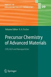
Material synthesis by the transformation of organometallic compounds (precursors) by vapor deposition techniques such as chemical vapor deposition (CVD) and atomic layer deposition (ALD) has been in the forefront of modern day research and development of new materials. There exists a need for new routes for designing and synthesizing new precursors as well as the application of established molecular precursors to derive tuneable materials for technological demands. With regard to the precursor chemistry, a most detailed understanding of the mechanistic complexity of materials formation from molecular precursors is very important for further development of new processes and advanced materials. To emphasize and stimulate research in these areas, this volume comprises a selection of case studies covering various key-aspects of the interplay of precursor chemistry with the process conditions of materials formation, particularly looking at the similarities and differences of CVD, ALD and nanoparticle synthesis, e.g. colloid chemistry, involving tailored molecular precursors.
Organometallic compounds --- Metal organic chemical vapor deposition --- Chemical vapor deposition --- Synthesis --- Metallo-organic compounds --- Metalloids, Organic --- Metalorganic compounds --- Organometalloids --- Organic compounds --- Metal organic vapor phase epitaxy --- Metallorganic vapor phase epitaxy --- MOCVD (Vapor deposition) --- MOVPE (Vapor deposition) --- OMCVD (Vapor deposition) --- OMVPE (Vapor deposition) --- Organo-metal vapor phase epitaxy --- Organometallic chemical vapor deposition --- Organometallic vapor phase epitaxy --- CVD (Chemical vapor deposition) --- Deposition, Chemical vapor --- Vapor deposition, Chemical --- Vapor-plating --- Organometallic compounds - Synthesis
Book
Year: 2021 Publisher: Basel, Switzerland MDPI - Multidisciplinary Digital Publishing Institute
Abstract | Keywords | Export | Availability | Bookmark
Loading...Choose an application
- Reference Manager
- EndNote
- RefWorks (Direct export to RefWorks)
Owing to their unique characteristics, direct wide bandgap energy, large breakdown field, and excellent electron transport properties, including operation at high temperature environments and low sensitivity to ionizing radiation, gallium nitride (GaN) and related group III-nitride heterostructures proved to be enabling materials for advanced optoelectronic and electronic devices and systems. Today, they are widely used in high performing short wavelength light emitting diodes (LEDs) and laser diodes (LDs), high performing radar, wireless telecommunications, as well ‘green’ power electronics. Impressive progress in GaN technology over the last 25 years has been driven by a continuously growing need for more advanced systems, and still new challenges arise and need to be solved. Actually, lighting industry, RF defene industry, and 5G mmWave telecommunication systems are driving forces for further intense research in order to reach full potential of GaN-based semiconductors. In the literature, there is a number of review papers and publications reporting technology progress and indicating future trends. In this Special Issue of Electronics, eight papers are published, the majority of them focusing materials and process technology of GaN-based devices fabricated on native GaN substrates. The specific topics include: GaN single crystalline substrates for electronic devices by ammonothermal and HVPE methods, Selective – Area Metalorganic Vapour – Phase Epitaxy of GaN and AlGaN/GaN hetereostructures for HEMTs, Advances in Ion Implantation of GaN and Related Materials including high pressure processing (lattice reconstruction) of ion implanted GaN (Mg and Be) and III-Nitride Nanowires for electronic and optoelectronic devices.
GaN HEMT --- self-heating effect --- microwave power amplifier --- thermal impedance --- thermal time constant --- thermal equivalent circuit --- GaN --- crystal growth --- ammonothermal method --- HVPE --- ion implantation --- gallium nitride --- thermodynamics --- ultra-high-pressure annealing --- diffusion --- diffusion coefficients --- molecular beam epitaxy --- nitrides --- laser diode --- tunnel junction --- LTE --- AlN --- AlGaN/GaN --- interface state density --- conductance-frequency --- MISHEMT --- gallium nitride nanowires --- polarity --- Kelvin probe force microscopy --- selective area growth --- selective epitaxy --- AlGaN/GaN heterostructures --- edge effects --- effective diffusion length --- MOVPE --- nanowires --- AlGaN --- LEDs --- growth polarity --- n/a
Book
Year: 2021 Publisher: Basel, Switzerland MDPI - Multidisciplinary Digital Publishing Institute
Abstract | Keywords | Export | Availability | Bookmark
Loading...Choose an application
- Reference Manager
- EndNote
- RefWorks (Direct export to RefWorks)
Owing to their unique characteristics, direct wide bandgap energy, large breakdown field, and excellent electron transport properties, including operation at high temperature environments and low sensitivity to ionizing radiation, gallium nitride (GaN) and related group III-nitride heterostructures proved to be enabling materials for advanced optoelectronic and electronic devices and systems. Today, they are widely used in high performing short wavelength light emitting diodes (LEDs) and laser diodes (LDs), high performing radar, wireless telecommunications, as well ‘green’ power electronics. Impressive progress in GaN technology over the last 25 years has been driven by a continuously growing need for more advanced systems, and still new challenges arise and need to be solved. Actually, lighting industry, RF defene industry, and 5G mmWave telecommunication systems are driving forces for further intense research in order to reach full potential of GaN-based semiconductors. In the literature, there is a number of review papers and publications reporting technology progress and indicating future trends. In this Special Issue of Electronics, eight papers are published, the majority of them focusing materials and process technology of GaN-based devices fabricated on native GaN substrates. The specific topics include: GaN single crystalline substrates for electronic devices by ammonothermal and HVPE methods, Selective – Area Metalorganic Vapour – Phase Epitaxy of GaN and AlGaN/GaN hetereostructures for HEMTs, Advances in Ion Implantation of GaN and Related Materials including high pressure processing (lattice reconstruction) of ion implanted GaN (Mg and Be) and III-Nitride Nanowires for electronic and optoelectronic devices.
Technology: general issues --- GaN HEMT --- self-heating effect --- microwave power amplifier --- thermal impedance --- thermal time constant --- thermal equivalent circuit --- GaN --- crystal growth --- ammonothermal method --- HVPE --- ion implantation --- gallium nitride --- thermodynamics --- ultra-high-pressure annealing --- diffusion --- diffusion coefficients --- molecular beam epitaxy --- nitrides --- laser diode --- tunnel junction --- LTE --- AlN --- AlGaN/GaN --- interface state density --- conductance-frequency --- MISHEMT --- gallium nitride nanowires --- polarity --- Kelvin probe force microscopy --- selective area growth --- selective epitaxy --- AlGaN/GaN heterostructures --- edge effects --- effective diffusion length --- MOVPE --- nanowires --- AlGaN --- LEDs --- growth polarity --- n/a
| Listing 1 - 5 of 5 |
Sort by
|