| Listing 1 - 10 of 12 | << page >> |
Sort by
|
Book
ISBN: 1283734265 0123918596 012387839X 0128121378 9780123918598 9781283734264 9780123878397 9780128121375 9780128121368 012812136X Year: 2012 Publisher: Amsterdam : Elsevier,
Abstract | Keywords | Export | Availability | Bookmark
 Loading...
Choose an application
- Reference Manager
- EndNote
- RefWorks (Direct export to RefWorks)
This multi-contributor handbook discusses Molecular Beam Epitaxy (MBE), an epitaxial deposition technique which involves laying down layers of materials with atomic thicknesses on to substrates. It summarizes MBE research and application in epitaxial growth with close discussion and a 'how to' on processing molecular or atomic beams that occur on a surface of a heated crystalline substrate in a vacuum. MBE has expanded in importance over the past thirty years (in terms of unique authors, papers and conferences) from a pure research domain into commercial applications (prototype devi
Molecular beam epitaxy. --- Nanotechnology. --- Optoelectronic devices - Materials. --- Optoelectronic devices -- Materials. --- Semiconductors - Materials. --- Semiconductors -- Materials. --- Semiconductors. --- Molecular beam epitaxy --- Optoelectronic devices --- Semiconductors --- Physics --- Physical Sciences & Mathematics --- Electricity & Magnetism --- Materials --- Materials. --- Photo electric devices --- Photo electronic devices --- Photoelectronic devices --- Electronic apparatus and appliances --- Optical instruments --- Electrooptical devices --- Integrated optics --- Epitaxy --- Molecular beams --- Photonic devices --- Photonic instruments
Book
ISBN: 1281795291 9786611795290 0080560474 0080463258 9780080560472 9780080463254 Year: 2008 Publisher: Oxford : Elsevier,
Abstract | Keywords | Export | Availability | Bookmark
 Loading...
Choose an application
- Reference Manager
- EndNote
- RefWorks (Direct export to RefWorks)
In 1969, Leo Esaki (1973 Nobel Laureate) and Ray Tsu from IBM, USA, proposed research on "man-made crystals? using a semiconductor superlattice (a semiconductor structure comprising several alternating ultra-thin layers of semiconductor materials with different properties). This invention was perhaps the first proposal to advocate the engineering of a new semiconductor material, and triggered a wide spectrum of experimental and theoretical investigations. However, the study of what are now called low dimensional structures (LDS) began in the late 1970's when sufficiently thin epitaxial layers
Nanostructured materials. --- Nanotechnology. --- Molecular technology --- Nanoscale technology --- High technology --- Nanomaterials --- Nanometer materials --- Nanophase materials --- Nanostructure controlled materials --- Nanostructure materials --- Ultra-fine microstructure materials --- Microstructure --- Nanotechnology
Book
ISBN: 012812136X Year: 2018 Publisher: Amsterdam : Elsevier,
Abstract | Keywords | Export | Availability | Bookmark
 Loading...
Choose an application
- Reference Manager
- EndNote
- RefWorks (Direct export to RefWorks)
Molecular beam epitaxy. --- Semiconductors --- Materials. --- Epitaxy --- Molecular beams

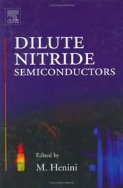
ISBN: 9780080445021 0080445020 9780080455990 0080455999 1280628340 9781280628344 9786610628346 Year: 2005 Publisher: Amsterdam : Elsevier,
Abstract | Keywords | Export | Availability | Bookmark
 Loading...
Choose an application
- Reference Manager
- EndNote
- RefWorks (Direct export to RefWorks)
* This book contains full account of the advances made in the dilute nitrides, providing an excellent starting point for workers entering the field. * It gives the reader easier access and better evaluation of future trends, Conveying important results and current ideas * Includes a generous list of references at the end of each chapter, providing a useful reference to the III-V-N based semiconductors research community. The high speed lasers operating at wavelength of 1.3 μm and 1.55 μm are very important light sources in optical communications since the optical fiber used as a transpo
Semiconductors. --- Nitrides. --- Heat resistant alloys --- Surface hardening --- Crystalline semiconductors --- Semi-conductors --- Semiconducting materials --- Semiconductor devices --- Crystals --- Electrical engineering --- Electronics --- Solid state electronics --- Materials
Digital
ISBN: 9780123918598 0123918596 9781283734264 1283734265 Year: 2013 Publisher: Amsterdam Elsevier
Abstract | Keywords | Export | Availability | Bookmark
 Loading...
Choose an application
- Reference Manager
- EndNote
- RefWorks (Direct export to RefWorks)
This multi-contributor handbook discusses Molecular Beam Epitaxy (MBE), an epitaxial deposition technique which involves laying down layers of materials with atomic thicknesses on to substrates. It summarizes MBE research and application in epitaxial growth with close discussion and a 'how to' on processing molecular or atomic beams that occur on a surface of a heated crystalline substrate in a vacuum. MBE has expanded in importance over the past thirty years (in terms of unique authors, papers and conferences) from a pure research domain into commercial applications (prototype device structures and more at the advanced research stage). MBE is important because it enables new device phenomena and facilitates the production of multiple layered structures with extremely fine dimensional and compositional control. The techniques can be deployed wherever precise thin-film devices with enhanced and unique properties for computing, optics or photonics are required. This book covers the advances made by MBE both in research and mass production of electronic and optoelectronic devices. It includes new semiconductor materials, new device structures which are commercially available, and many more which are at the advanced research stage. Condenses fundamental science of MBE into a modern reference, speeding up literature reviewDiscusses new materials, novel applications and new device structures, grounding current commercial applications with modern understanding in industry and research Coverage of MBE as mass production epitaxial technology enhances processing efficiency and throughput for semiconductor industry and nanostructured semiconductor materials research community.
Digital
ISBN: 9780128121375 0128121378 9780128121368 012812136X Year: 2018 Publisher: Amsterdam, Netherlands Elsevier
Abstract | Keywords | Export | Availability | Bookmark
 Loading...
Choose an application
- Reference Manager
- EndNote
- RefWorks (Direct export to RefWorks)
Molecular Beam Epitaxy (MBE): From Research to Mass Production, Second Edition, provides a comprehensive overview of the latest MBE research and applications in epitaxial growth, along with a detailed discussion and 'how to' on processing molecular or atomic beams that occur on the surface of a heated crystalline substrate in a vacuum. The techniques addressed in the book can be deployed wherever precise thin-film devices with enhanced and unique properties for computing, optics or photonics are required. It includes new semiconductor materials, new device structures that are commercially available, and many that are at the advanced research stage. This second edition covers the advances made by MBE, both in research and in the mass production of electronic and optoelectronic devices. Enhancements include new chapters on MBE growth of 2D materials, Si-Ge materials, AIN and GaN materials, and hybrid ferromagnet and semiconductor structures.

ISBN: 9780080445021 0080445020 9780080455990 0080455999 1280628340 9781280628344 Year: 2005 Publisher: London Elsevier
Abstract | Keywords | Export | Availability | Bookmark
 Loading...
Choose an application
- Reference Manager
- EndNote
- RefWorks (Direct export to RefWorks)
* This book contains full account of the advances made in the dilute nitrides, providing an excellent starting point for workers entering the field. * It gives the reader easier access and better evaluation of future trends, Conveying important results and current ideas * Includes a generous list of references at the end of each chapter, providing a useful reference to the III-V-N based semiconductors research community. The high speed lasers operating at wavelength of 1.3 æm and 1.55 æm are very important light sources in optical communications since the optical fiber used as a transport media of light has dispersion and attenuation minima, respectively, at these wavelengths. These long wavelengths are exclusively made of InP-based material InGaAsP/InP. However, there are several problems with this material system. Therefore, there has been considerable effort for many years to fabricate long wavelength laser structures on other substrates, especially GaAs. The manufacturing costs of GaAs-based components are lower and the processing techniques are well developed. In 1996 a novel quaternary material GaInAsN was proposed which could avoid several problems with the existing technology of long wavelength lasers. In this book, several leaders in the field of dilute nitrides will cover the growth and processing, experimental characterization, theoretical understanding, and device design and fabrication of this recently developed class of semiconductor alloys. They will review their current status of research and development. Dilute Nitrides (III-N-V) Semiconductors: Physics and Technology organises the most current available data, providing a ready source of information on a wide range of topics, making this book essential reading for all post graduate students, researchers and practitioners in the fields of Semiconductors and Optoelectronics * This book contains full account of the advances made in the dilute nitrides, providing an excellent starting point for workers entering the field. * It gives the reader easier access and better evaluation of future trends, Conveying important results and current ideas * Includes a generous list of references at the end of each chapter, providing a useful reference to the III-V-N based semiconductors research community.
Multi
ISBN: 9780080560472 0080560474 9780080463254 0080463258 1281795291 9786611795290 Year: 2008 Publisher: Oxford : Elsevier,
Abstract | Keywords | Export | Availability | Bookmark
 Loading...
Choose an application
- Reference Manager
- EndNote
- RefWorks (Direct export to RefWorks)
In 1969, Leo Esaki (1973 Nobel Laureate) and Ray Tsu from IBM, USA, proposed research on "man-made crystals? using a semiconductor superlattice (a semiconductor structure comprising several alternating ultra-thin layers of semiconductor materials with different properties). This invention was perhaps the first proposal to advocate the engineering of a new semiconductor material, and triggered a wide spectrum of experimental and theoretical investigations. However, the study of what are now called low dimensional structures (LDS) began in the late 1970's when sufficiently thin epitaxial layers
Mechanical properties of solids --- Materials sciences --- Nanostructured materials. --- Nanotechnology.

ISBN: 1281060305 9786611060305 0080507913 1856173887 9781856173889 9780080507910 9781281060303 Year: 2002 Publisher: New York Elsevier Advanced Technology
Abstract | Keywords | Export | Availability | Bookmark
 Loading...
Choose an application
- Reference Manager
- EndNote
- RefWorks (Direct export to RefWorks)
The use of lasers which emit infra-red radiation and sophisticated detectors of IR radiation is increasing dramatically: they are being used for long-distance fibre-optic communications and remote environmental monitoring and sensing. Thus they are of interest to the telecommunications industry and the military in particular. This book has been designed to bring together what is known on these devices, using an international group of contributors.

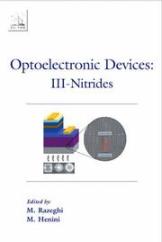
ISBN: 0080538118 0080444261 9780080538112 9780080444260 Year: 2004 Publisher: Amsterdam San Diego Oxford Elsevier
Abstract | Keywords | Export | Availability | Bookmark
 Loading...
Choose an application
- Reference Manager
- EndNote
- RefWorks (Direct export to RefWorks)
Optoelectronic devices --- Testing. --- Research. --- Photo electric devices --- Photo electronic devices --- Photoelectronic devices --- Electronic apparatus and appliances --- Optical instruments --- Electrooptical devices --- Integrated optics --- Photonic devices --- Photonic instruments
| Listing 1 - 10 of 12 | << page >> |
Sort by
|

 Search
 Feedback
 About UniCat
  Help
Help News
News