| Listing 1 - 9 of 9 |
Sort by
|
Book
Year: 2008 Publisher: Adelphi, Md. : Army Research Laboratory,
Abstract | Keywords | Export | Availability | Bookmark
 Loading...
Choose an application
- Reference Manager
- EndNote
- RefWorks (Direct export to RefWorks)
Book
ISBN: 1281960896 9786611960896 9812812059 9789812812056 9789812568649 9812568646 9781281960894 6611960899 Year: 2008 Publisher: Singapore Hackensack, N.J. World Scientific Pub.
Abstract | Keywords | Export | Availability | Bookmark
 Loading...
Choose an application
- Reference Manager
- EndNote
- RefWorks (Direct export to RefWorks)
This volume provides a timely description of the latest compact MOS transistor models for circuit simulation. The first generation BSIM3 and BSIM4 models that have dominated circuit simulation in the last decade are no longer capable of characterizing all the important features of modern sub-100nm MOS transistors. This book discusses the second generation MOS transistor models that are now in urgent demand and being brought into the initial phase of manufacturing applications. It considers how the models are to include the complete drift-diffusion theory using the surface potential variable in the MOS transistor channel in order to give one characterization equation.
Book
ISBN: 9780470229415 Year: 2008 Publisher: Hoboken Wiley
Abstract | Keywords | Export | Availability | Bookmark
 Loading...
Choose an application
- Reference Manager
- EndNote
- RefWorks (Direct export to RefWorks)

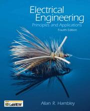
ISBN: 0131989227 9780131989221 0132066920 9780132066921 0136138837 0136138845 9780136138839 9780136138846 Year: 2008 Publisher: Upper Saddle River Pearson Prentice Hall
Abstract | Keywords | Export | Availability | Bookmark
 Loading...
Choose an application
- Reference Manager
- EndNote
- RefWorks (Direct export to RefWorks)
electrical engineering --- Electrical engineering --- Electric engineering --- Electric engineering. --- elektriciteit --- schakelingen --- inductie --- diodes --- versterkers --- transistors --- Engineering
Book
ISBN: 9782100516131 Year: 2008 Publisher: Paris : Dunod,
Abstract | Keywords | Export | Availability | Bookmark
 Loading...
Choose an application
- Reference Manager
- EndNote
- RefWorks (Direct export to RefWorks)
Electronics --- Electronic circuits --- Electronique --- Circuits électroniques --- Problems, exercices, etc --- Handbooks, manuals, etc --- Problèmes et exercices --- Guides, manuels, etc --- Électronique --- Circuits électroniques --- Problèmes et exercices --- Problems, exercices, etc. --- Électronique. --- Amplificateurs différentiels. --- Differential amplifiers --- Transistor amplifiers --- Amplificateurs à transistors. --- Électronique. --- Amplificateurs différentiels. --- Amplificateurs à transistors.

ISBN: 1281087637 9786611087630 0387717528 038771751X 1441944095 9780387717517 9780387717524 Year: 2008 Publisher: Boston, MA Springer Science+Business Media, LLC
Abstract | Keywords | Export | Availability | Bookmark
 Loading...
Choose an application
- Reference Manager
- EndNote
- RefWorks (Direct export to RefWorks)
FinFETs and Other Multi-Gate Transistors provides a comprehensive description of the physics, technology and circuit applications of multigate field-effect transistors (FETs). It explains the physics and properties of these devices, how they are fabricated and how circuit designers can use them to improve the performances of integrated circuits. The International Technology Roadmap for Semiconductors (ITRS) recognizes the importance of these devices and places them in the "Advanced non-classical CMOS devices" category. Of all the existing multigate devices, the FinFET is the most widely known. FinFETs and Other Multi-Gate Transistors is dedicated to the different facets of multigate FET technology and is written by leading experts in the field.
Transistors. --- Electronics. --- Electrical engineering --- Physical sciences --- Electronics --- Semiconductors --- Metal oxide semiconductor field-effect transistors. --- Silicon-on-insulator technology. --- Transistors MOSFET --- Silicium sur isolant --- EPUB-LIV-FT SPRINGER-B LIVINGEN --- Systems engineering. --- Engineering. --- Computer engineering. --- Circuits and Systems. --- Electronics and Microelectronics, Instrumentation. --- Engineering, general. --- Electrical Engineering. --- Computers --- Construction --- Industrial arts --- Technology --- Engineering systems --- System engineering --- Engineering --- Industrial engineering --- System analysis --- Design and construction --- Electronic circuits. --- Microelectronics. --- Electrical engineering. --- Electric engineering --- Microminiature electronic equipment --- Microminiaturization (Electronics) --- Microtechnology --- Miniature electronic equipment --- Electron-tube circuits --- Electric circuits --- Electron tubes

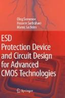
ISBN: 1281397946 9786611397944 1402083017 1402083009 9048178363 Year: 2008 Publisher: [Dordrecht] : Springer,
Abstract | Keywords | Export | Availability | Bookmark
 Loading...
Choose an application
- Reference Manager
- EndNote
- RefWorks (Direct export to RefWorks)
The challenges associated with the design and implementation of Electrostatic Discharge (ESD) protection circuits are becoming increasingly complex as technology is scaled well into nano-metric regime. Traditional approaches of ESD design may not be adequate as the ESD damages occur at successively lower voltages in nano-metric dimensions. There are several challenges that must be met in order to design robust ESD circuits today. Due to technology scaling and proliferation of automated handling, ESD failures in ICs caused by Charged Device Model (CDM) are increasing. CDM discharges can cause latent damages which could degrade and eventually lead to definite failures in the ICs. The ESD protection design for current and future sub-65nm CMOS circuits is a challenge for high I/O count, multiple power domains and flip-chip products. ESD Protection Device and Circuit Design for Advanced CMOS Technologies is intended for practicing engineers working in the areas of circuit design, VLSI reliability and testing domains. As the problems associated with ESD failures and yield losses become significant in the modern semiconductor industry, the demand for graduates with a basic knowledge of ESD is also increasing. Today, there is a significant demand to educate the circuits design and reliability teams on ESD issues. This book makes an attempt to address the ESD design and implementation in a systematic manner. A design procedure involving device simulators as well as circuit simulator is employed to optimize device and circuit parameters for optimal ESD as well as circuit performance. This methodology, described in ESD Protection Device and Circuit Design for Advanced CMOS Technologies has resulted in several successful ESD circuit design with excellent silicon results demonstrates its strengths.
Integrated circuits --- Electronic apparatus and appliances --- Electric discharges. --- Metal oxide semiconductors, Complementary --- Metal oxide semiconductor field-effect transistors. --- Protection. --- Design and construction. --- MOSFET --- Field-effect transistors --- Metal oxide semiconductors --- Discharges (Electricity) --- Electricity --- Electrostatic discharges --- Electrostatics --- Nuclear physics --- Electric action of points --- Photoelectricity --- Electronic packaging --- Chips (Electronics) --- Circuits, Integrated --- Computer chips --- Microchips --- Electronic circuits --- Microelectronics --- Discharges --- Electronics. --- Systems engineering. --- Optical materials. --- Electronics and Microelectronics, Instrumentation. --- Circuits and Systems. --- Optical and Electronic Materials. --- Solid State Physics. --- Spectroscopy and Microscopy. --- Electrical engineering --- Physical sciences --- Optics --- Materials --- Engineering systems --- System engineering --- Engineering --- Industrial engineering --- System analysis --- Design and construction --- Microelectronics. --- Electronic circuits. --- Electronic materials. --- Solid state physics. --- Spectroscopy. --- Microscopy. --- Analysis, Microscopic --- Light microscopy --- Micrographic analysis --- Microscope and microscopy --- Microscopic analysis --- Optical microscopy --- Analysis, Spectrum --- Spectra --- Spectrochemical analysis --- Spectrochemistry --- Spectrometry --- Spectroscopy --- Chemistry, Analytic --- Interferometry --- Radiation --- Wave-motion, Theory of --- Absorption spectra --- Light --- Spectroscope --- Physics --- Solids --- Electronic materials --- Electron-tube circuits --- Electric circuits --- Electron tubes --- Electronics --- Microminiature electronic equipment --- Microminiaturization (Electronics) --- Microtechnology --- Semiconductors --- Miniature electronic equipment --- Qualitative --- Analytical chemistry
Periodical
Abstract | Keywords | Export | Availability | Bookmark
 Loading...
Choose an application
- Reference Manager
- EndNote
- RefWorks (Direct export to RefWorks)
Electronics --- Electronic apparatus and appliances --- Composants électroniques --- Periodicals. --- Périodiques --- Electronic apparatus and appliances. --- Engineering --- Coatings and Films --- General and Others --- Nanomaterials --- Solid State Physics --- Material Science and Metallurgy --- Physics --- Engineering. --- Solid State Physics. --- Material Science and Metallurgy. --- Physics. --- transistors --- integrated circuits --- semiconductor materials --- thick-film materials --- capacitors --- solid-state memories --- Electronic devices --- Physical instruments --- Scientific apparatus and instruments --- Electronic instruments --- Apparatus and appliances --- Nuclear energy --- kernenergie
Book
ISBN: 1402064810 1402064802 Year: 2008 Publisher: Dordrecht : Springer Netherlands : Imprint: Springer,
Abstract | Keywords | Export | Availability | Bookmark
 Loading...
Choose an application
- Reference Manager
- EndNote
- RefWorks (Direct export to RefWorks)
Semiconductor Device Physics and Design provides a fresh and unique teaching tool. Over the last decade device performances are driven by new materials, scaling, heterostructures and new device concepts. Semiconductor devices have mostly relied on Si but increasingly GaAs, InGaAs and heterostructures made from Si/SiGe, GaAs/AlGaAs etc have become important. Over the last few years one of the most exciting new entries has been the nitride based heterostructures. New physics based on polar charges and polar interfaces has become important as a result of the nitrides. Nitride based devices are now used for high power applications and in lighting and display applications. For students to be able to participate in this exciting arena, a lot of physics, device concepts, heterostructure concepts and materials properties need to be understood. It is important to have a textbook that teaches students and practicing engineers about all these areas in a coherent manner. Semiconductor Device Physics and Design starts out with basic physics concepts including the physics behind polar heterostructures and strained heterostructures. Important devices ranging from p-n diodes to bipolar and field effect devices are then discussed. An important distinction users will find in this book is the discussion presented on device needs from the perspective of various technologies. For example, how much gain is needed in a transistor, how much power, what kind of device characteristics is needed? Not surprisingly the needs depend upon applications. The needs of an A/D or D/A converter will be different from that of an amplifier in a cell phone. Similarly the diodes used in a laptop will place different requirements on the device engineer than diodes used in a mixer circuit. By relating device design to device performance and then relating device needs to system use the student can see how device design works in real world. < Semiconductor Device Physics and Design is comprehensive without being overwhelming. The focus was to make this a useful text book so that the information contained is cohesive without including all aspects of device physics. The lesson plans demonstrated how this book could be used in a 1 semester or 2 quarter sequence.
Semiconductors. --- Transistors. --- Electronics --- Semiconductors --- Crystalline semiconductors --- Semi-conductors --- Semiconducting materials --- Semiconductor devices --- Crystals --- Electrical engineering --- Solid state electronics --- Materials --- Systems engineering. --- Optical materials. --- Circuits and Systems. --- Solid State Physics. --- Spectroscopy and Microscopy. --- Optical and Electronic Materials. --- Optics --- Engineering systems --- System engineering --- Engineering --- Industrial engineering --- System analysis --- Design and construction --- Electronic circuits. --- Solid state physics. --- Spectroscopy. --- Microscopy. --- Electronic materials. --- Electronic materials --- Analysis, Microscopic --- Light microscopy --- Micrographic analysis --- Microscope and microscopy --- Microscopic analysis --- Optical microscopy --- Analysis, Spectrum --- Spectra --- Spectrochemical analysis --- Spectrochemistry --- Spectrometry --- Spectroscopy --- Chemistry, Analytic --- Interferometry --- Radiation --- Wave-motion, Theory of --- Absorption spectra --- Light --- Spectroscope --- Physics --- Solids --- Electron-tube circuits --- Electric circuits --- Electron tubes --- Qualitative --- Analytical chemistry
| Listing 1 - 9 of 9 |
Sort by
|

 Search
 Feedback
 About UniCat
  Help
Help News
News