| Listing 1 - 10 of 13 | << page >> |
Sort by
|
ISBN: 030648210X 1402070535 Year: 2002 Publisher: Boston, MA : Springer US,
Abstract | Keywords | Export | Availability | Bookmark
 Loading...
Choose an application
- Reference Manager
- EndNote
- RefWorks (Direct export to RefWorks)
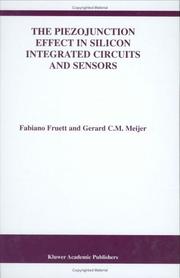
Mechanical stress affects the magnitude of base-emitter voltages of forward biased bipolar transistors. This phenomenon is called the piezojunction effect. The piezojunction effect is the main cause of inaccuracy and drift in integrated temperature sensors and bandgap voltage references. The aim of The Piezojunction Effect in Silicon Integrated Circuits and Sensors is twofold. Firstly, to describe techniques that can reduce the mechanical-stress-induced inaccuracy and long-term instability. Secondly, to show, that the piezojunction effect can be applied for new types of mechanical-sensor structures. During IC fabrication and packaging thermo-mechanical stress is induced, when the packaged chips cool down to the temperature of application. The piezojunction effect is caused by a stress-induced change in the conductivity of the minority-charge carriers, while the piezoresistive effect is caused by a similar effect for the majority-charge carriers. To characterise the anisotropic piezojunction effect, the authors performed systematic investigations over wide ranges of mechanical stress and temperature. The experiments have been performed for various crystal and stress orientations. The experimental results have been used to extract the first- and second-order piezojunction (FOPJ and SOPJ) coefficients for bipolar transistors. It is shown how the knowledge of the piezojunction and piezoresistive coefficients can used to minimize the undesirable mechanical-stress effects on the electrical characteristics of transistors and resistors, respectively. Devices with lower mechanical-stress sensitivity can be found by comparing their piezo-coefficients. The layout of the device can also be optimized to reduce the mechanical-stress sensitivity. As a next step it is shown, how the knowledge of the piezo-effects on device level can be used to predict and to reduce their negative influence on circuit level. This is demonstrated for a number of important basic circuits, including translinear circuits, temperature transducers and bandgap references. Finally, it is shown how the piezojunction effect can be used to fabricate stress-sensing elements. It appears that, in comparison with resistive stress-sensing elements, the piezojunction sensors have the advantage of a smaller size and very low power dissipation.
Engineering. --- Electrical engineering. --- Electronic circuits. --- Optical materials. --- Electronic materials. --- Circuits and Systems. --- Electrical Engineering. --- Optical and Electronic Materials. --- Electronic materials --- Optics --- Materials --- Electron-tube circuits --- Electric circuits --- Electron tubes --- Electronics --- Electric engineering --- Engineering --- Construction --- Industrial arts --- Technology --- Materials.
ISBN: 3540421769 3642075770 366205003X Year: 2002 Publisher: Berlin Springer
Abstract | Keywords | Export | Availability | Bookmark
 Loading...
Choose an application
- Reference Manager
- EndNote
- RefWorks (Direct export to RefWorks)
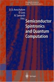
The manipulation of electric charge in bulk semiconductors and their heterostructures forms the basis of virtually all contemporary electronic and opto-electronic devices. Recent studies of spin-dependent phenomena in semiconductors have now opened the door to technological possibilities that harness the spin of the electron in semiconductor devices. In addition to providing spin-dependent analogies that extend existing electronic devices into the realm of semiconductor "spintronics," the spin degree of freedom also offers prospects for fundamentally new functionality within the quantum domain, ranging from storage to computation. It is anticipated that the spin degree of freedom in semiconductors will play a crucial role in the development of information technologies in the 21st century. This book brings together a team of experts to provide an overview of emerging concepts in this rapidly developing field. The topics range from spin transport and injection in semiconductors and their heterostructures to coherent processes and computation in semiconductor quantum structures and microcavities.
Quantum mechanics. Quantumfield theory --- Logic devices --- Quantum electronics --- Spintronics --- Magnetoelectronics --- Spin electronics --- Microelectronics --- Nanotechnology --- Electronics --- Quantum electrodynamics --- Electronic apparatus and appliances --- Fluxtronics --- Spinelectronics --- Nanotechnology. --- Optical materials. --- Electronic materials. --- Magnetism. --- Magnetic materials. --- Optical and Electronic Materials. --- Magnetism, Magnetic Materials. --- Materials --- Mathematical physics --- Physics --- Electricity --- Magnetics --- Molecular technology --- Nanoscale technology --- High technology --- Electronic materials --- Optics --- Semiconductor compounds --- Solid state
ISBN: 0792375874 1461352800 1461508711 Year: 2002 Publisher: Boston (Mass.) : Kluwer academic,
Abstract | Keywords | Export | Availability | Bookmark
 Loading...
Choose an application
- Reference Manager
- EndNote
- RefWorks (Direct export to RefWorks)
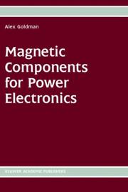
Magnetic Components for Power Electronics concerns the important considerations necessary in the choice of the optimum magnetic component for power electronic applications. These include the topology of the converter circuit, the core material, shape, size and others such as cost and potential component suppliers. These are all important for the design engineer due to the emergence of new materials, changes in supplier management and the examples of several component choices. Suppliers using this volume will also understand the needs of designers. Highlights include: Emphasis on recently introduced new ferrite materials, such as those operating at megahertz frequencies and under higher DC drive conditions; Discussion of amorphous and nanocrystalline metal materials; New technologies such as resonance converters, power factors correction (PFC) and soft switching; Catalog information from over 40 magnetic component suppliers; Examples of methods of component choice for ferrites, amorphous nanocrystalline materials; Information on suppliers management changes such as those occurring at Siemens, Philips, Thomson and Allied-Signal; Attention to the increasingly important concerns about EMI. This book should be especially helpful for power electronic circuit designers, technical executives, and material science engineers involved with power electronic components.
Electric power supplies to apparatus --- -Magnets --- Electric coils --- -Coils, Electric --- Magnetic circuits --- Tank circuits --- Magnetic materials --- Magnetics --- Magnetism --- Solenoids --- Power supplies to apparatus, Electric --- Electric power --- Equipment and supplies --- -Materials --- Materials --- Magnets. --- Materials. --- -Equipment and supplies --- Magnets --- Coils, Electric --- Equipment and supplies&delete& --- Electrical engineering. --- Optical materials. --- Electronic materials. --- Electrical Engineering. --- Optical and Electronic Materials. --- Electronic materials --- Optics --- Electric engineering --- Engineering
Book
ISBN: 1280200405 9786610200405 0306475537 Year: 2002 Publisher: Norwell, Massachusetts : Kluwer Academic Publishers,
Abstract | Keywords | Export | Availability | Bookmark
 Loading...
Choose an application
- Reference Manager
- EndNote
- RefWorks (Direct export to RefWorks)
Emerging Memories: Technologies and Trends attempts to provide background and a description of the basic technology, function and properties of emerging as well as discussing potentially suitable applications. This book explores a range of new memory products and technologies. The concept for some of these memories has been around for years. A few completely new. Some involve materials that have been in volume production in other type of devices for some time. Ferro-electrics, for example, have been used in capacitors for more than 30 years. In addition to looking at using known devices and materials in novel ways, there are new technologies being investigated such as DNA memories, light memories, molecular memories, and carbon nanotube memories, as well as the new polymer memories which hold the potential for the significant manufacturing reduction. Emerging Memories: Technologies and Trends is a useful reference for the professional engineer in the semiconductor industry.
Computer storage devices. --- Semiconductor storage devices. --- Systems engineering. --- Computer engineering. --- Optical materials. --- Circuits and Systems. --- Electrical Engineering. --- Optical and Electronic Materials. --- Electronic circuits. --- Electrical engineering. --- Electronic materials. --- Electronic materials --- Optics --- Materials --- Electric engineering --- Engineering --- Electron-tube circuits --- Electric circuits --- Electron tubes --- Electronics
ISBN: 1280206535 9786610206537 0306470829 0306459485 Year: 2002 Publisher: New York, NY : Springer US : Imprint: Springer,
Abstract | Keywords | Export | Availability | Bookmark
 Loading...
Choose an application
- Reference Manager
- EndNote
- RefWorks (Direct export to RefWorks)
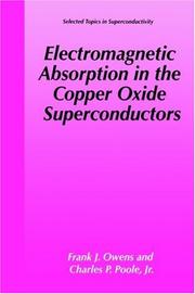
In 1987 a major breakthrough occurred in materials science. A new family of materials was discovered that became superconducting above the temperature at which nitrogen gas liquifies, namely, 77 K or –196°C. Within months of the discovery, a wide variety of experimental techniques were brought to bear in order to measure the properties of these materials and to gain an understanding of why they superconduct at such high temperatures. Among the techniques used were electromagnetic absorption in both the normal and the superconducting states. The measurements enabled the determination of a wide variety of properties, and in some instances led to the observation of new effects not seen by other measu- ments, such as the existence of weak-link microwave absorption at low dc magnetic fields. The number of different properties and the degree of detail that can be obtained from magnetic field- and temperature-dependent studies of electromagnetic abso- tion are not widely appreciated. For example, these measurements can provide information on the band gap, critical fields, the H–T irreversibility line, the amount of trapped flux, and even information about the symmetry of the wave function of the Cooper pairs. It is possible to use low dc magnetic field-induced absorption of microwaves with derivative detection to verify the presence of superconductivity in a matter of minutes, and the measurements are often more straightforward than others. For example, they do not require the physical contact with the sample that is necessary when using four-probe resistivity to detect superconductivity.
Copper oxide superconductors. --- Electromagnetic waves. --- Surfaces (Physics). --- Optical materials. --- Characterization and Evaluation of Materials. --- Condensed Matter Physics. --- Optical and Electronic Materials. --- Optics --- Materials --- Physics --- Surface chemistry --- Surfaces (Technology) --- Materials science. --- Condensed matter. --- Electronic materials. --- Electronic materials --- Condensed materials --- Condensed media --- Condensed phase --- Materials, Condensed --- Media, Condensed --- Phase, Condensed --- Liquids --- Matter --- Solids --- Material science --- Physical sciences --- Electronics --- Materials.
ISBN: 1280200553 9780306475677 9786610200559 0306475677 0792376293 1475776438 9781280200557 9780306475672 Year: 2002 Publisher: Boston : Kluwer Academic Publishers,
Abstract | Keywords | Export | Availability | Bookmark
 Loading...
Choose an application
- Reference Manager
- EndNote
- RefWorks (Direct export to RefWorks)
Fundamentals of Solid State Engineering is structured in two major parts. It first addresses the basic physics concepts, which are at the base of solid state matter in general and semiconductors in particular. The second part reviews the technology for modern Solid State Engineering. This includes a review of compound semiconductor bulk and epitaxial thin films growth techniques, followed by a description of current semiconductor device processing and nano-fabrication technologies. A few examples of semiconductor devices and a description of their theory of operational are then discussed, including transistors, semiconductor lasers, and photodetectors.
Solid state electronics. --- Superconductors. --- Computer engineering. --- Optical materials. --- Electrical Engineering. --- Solid State Physics. --- Spectroscopy and Microscopy. --- Optical and Electronic Materials. --- Electrical engineering. --- Solid state physics. --- Spectroscopy. --- Microscopy. --- Electronic materials. --- Electronic materials --- Optics --- Materials --- Analysis, Microscopic --- Light microscopy --- Micrographic analysis --- Microscope and microscopy --- Microscopic analysis --- Optical microscopy --- Analysis, Spectrum --- Spectra --- Spectrochemical analysis --- Spectrochemistry --- Spectrometry --- Spectroscopy --- Chemistry, Analytic --- Interferometry --- Radiation --- Wave-motion, Theory of --- Absorption spectra --- Light --- Spectroscope --- Physics --- Solids --- Electric engineering --- Engineering --- Qualitative --- Analytical chemistry
ISBN: 0306483718 038723814X 030647249X 0387335528 Year: 2002 Publisher: New York, NY : Springer US : Imprint: Springer,
Abstract | Keywords | Export | Availability | Bookmark
 Loading...
Choose an application
- Reference Manager
- EndNote
- RefWorks (Direct export to RefWorks)
These books, with of a total of 40 chapters, are a comprehensive and complete introductory text on the synthesis, characterization, and applications of nanomaterials. They are aimed at graduate students and researchers whose background is chemistry, physics, materials science, chemical engineering, electrical engineering, and biomedical science. The first part emphasizes the chemical and physical approaches used for synthesis of nanomaterials. The second part emphasizes the techniques used for characterizing the structure and properties of nanomaterials, aiming at describing the physical mechanism, data interpretation, and detailed applications of the techniques. The final part focuses on systems of different nanostructural materials with novel properties and applications.
Materials science. --- Physical chemistry. --- Optical materials. --- Electronic materials. --- Materials Science. --- Characterization and Evaluation of Materials. --- Optical and Electronic Materials. --- Physical Chemistry. --- Surfaces (Physics). --- Chemistry, Physical organic. --- Chemistry, Physical organic --- Chemistry, Organic --- Chemistry, Physical and theoretical --- Optics --- Materials --- Physics --- Surface chemistry --- Surfaces (Technology) --- Nanostructured materials --- Chemistry, Theoretical --- Physical chemistry --- Theoretical chemistry --- Chemistry --- Electronic materials --- Material science --- Physical sciences --- Characterization and Analytical Technique. --- Optical Materials. --- Analysis. --- Chemistry, Physical and theoretical.
ISBN: 9401003416 140200561X 1402005601 Year: 2002 Volume: v. 57 Publisher: Dordrecht ; Boston ; London Brussels Kluwer Academic Publishers NATO Scientific Affairs Division
Abstract | Keywords | Export | Availability | Bookmark
 Loading...
Choose an application
- Reference Manager
- EndNote
- RefWorks (Direct export to RefWorks)
Nanostructures --- Nanotechnology --- Physics --- Physical Sciences & Mathematics --- Atomic Physics --- Nanostructures. --- Nanotechnology. --- Nanotechnologie --- Atoms. --- Physics. --- Condensed matter. --- Optical materials. --- Electronic materials. --- Polymers . --- Physical chemistry. --- Atomic, Molecular, Optical and Plasma Physics. --- Nanotechnology and Microengineering. --- Condensed Matter Physics. --- Optical and Electronic Materials. --- Polymer Sciences. --- Physical Chemistry. --- Chemistry, Theoretical --- Physical chemistry --- Theoretical chemistry --- Chemistry --- Polymere --- Polymeride --- Polymers and polymerization --- Macromolecules --- Electronic materials --- Optics --- Materials --- Condensed materials --- Condensed media --- Condensed phase --- Materials, Condensed --- Media, Condensed --- Phase, Condensed --- Liquids --- Matter --- Solids --- Molecular technology --- Nanoscale technology --- High technology --- Natural philosophy --- Philosophy, Natural --- Physical sciences --- Dynamics --- Chemistry, Physical and theoretical --- Stereochemistry --- Constitution
ISBN: 140200575X 1402005768 9401003394 9781402005763 9781402005756 Year: 2002 Volume: 58 Publisher: Dordrecht: Kluwer,
Abstract | Keywords | Export | Availability | Bookmark
 Loading...
Choose an application
- Reference Manager
- EndNote
- RefWorks (Direct export to RefWorks)
A review of the electrical properties, performance and physical mechanisms of the main silicon-on-insulator (SOI) materials and devices. Particular attention is paid to the reliability of SOI structures operating in harsh conditions. The first part of the book deals with material technology and describes the SIMOX and ELTRAN technologies, the smart-cut technique, SiCOI structures and MBE growth. The second part covers reliability of devices operating under extreme conditions, with an examination of low and high temperature operation of deep submicron MOSFETs and novel SOI technologies and circuits, SOI in harsh environments and the properties of the buried oxide. The third part deals with the characterization of advanced SOI materials and devices, covering laser-recrystallized SOI layers, ultrashort SOI MOSFETs and nanostructures, gated diodes and SOI devices produced by a variety of techniques. The last part reviews future prospects for SOI structures, analyzing wafer bonding techniques, applications of oxidized porous silicon, semi-insulating silicon materials, self-organization of silicon dots and wires on SOI and some new physical phenomena.
Semiconductors --- Silicon-on-insulator technology --- Extreme environments --- Semiconducteurs --- Silicium sur isolant --- Milieux extrêmes --- Congresses. --- Congresses --- Congrès --- Electrical & Computer Engineering --- Engineering & Applied Sciences --- Electrical Engineering --- Electronic circuits. --- Electronics. --- Microelectronics. --- Electrical engineering. --- Optical materials. --- Electronic materials. --- Materials science. --- Circuits and Systems. --- Electronics and Microelectronics, Instrumentation. --- Electrical Engineering. --- Optical and Electronic Materials. --- Characterization and Evaluation of Materials. --- Material science --- Physical sciences --- Electronic materials --- Optics --- Materials --- Electric engineering --- Engineering --- Microminiature electronic equipment --- Microminiaturization (Electronics) --- Electronics --- Microtechnology --- Miniature electronic equipment --- Electrical engineering --- Electron-tube circuits --- Electric circuits --- Electron tubes --- Semiconductors - Congresses --- Silicon-on-insulator technology - Congresses --- Extreme environments - Congresses
ISBN: 3540433937 3642077781 3662049740 Year: 2002 Publisher: Berlin ; New York, NY : Springer,
Abstract | Keywords | Export | Availability | Bookmark
 Loading...
Choose an application
- Reference Manager
- EndNote
- RefWorks (Direct export to RefWorks)
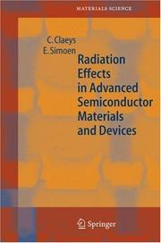
In the modern semiconductor industry, there is a growing need to understand and combat potential radiation damage problems. Space applications are an obvious case, but, beyond that, today's device and circuit fabrication rely on increasing numbers of processing steps that involve an aggressive environment where inadvertant radiation damage can occur. This book is both aimed at post-graduate researchers seeking an overview of the field, and will also be immensely useful for nuclear and space engineers and even process engineers. A background knowledge of semiconductor and device physics is assumed, but the basic concepts are all briefly summarized. Finally the book outlines the shortcomings of present experimental and modeling techniques and gives an outlook on future developments.
Semiconductors --- Effect of radiation on. --- -Crystalline semiconductors --- Semi-conductors --- Semiconducting materials --- Semiconductor devices --- Crystals --- Electrical engineering --- Electronics --- Solid state electronics --- Effect of radiation on --- Materials --- -Effect of radiation on --- Semiconductors, Effect of radiation on --- Crystallography. --- Energy policy. --- Energy and state. --- Optics. --- Electrodynamics. --- Materials science. --- Optical materials. --- Electronic materials. --- Materials—Surfaces. --- Thin films. --- Crystallography and Scattering Methods. --- Energy Policy, Economics and Management. --- Classical Electrodynamics. --- Characterization and Evaluation of Materials. --- Optical and Electronic Materials. --- Surfaces and Interfaces, Thin Films. --- Films, Thin --- Solid film --- Solids --- Surfaces (Technology) --- Coatings --- Thick films --- Electronic materials --- Optics --- Material science --- Physical sciences --- Dynamics --- Physics --- Light --- Energy and state --- Power resources --- State and energy --- Industrial policy --- Energy conservation --- Leptology --- Mineralogy --- Government policy
| Listing 1 - 10 of 13 | << page >> |
Sort by
|

 Search
 Feedback
 About UniCat
  Help
Help News
News